
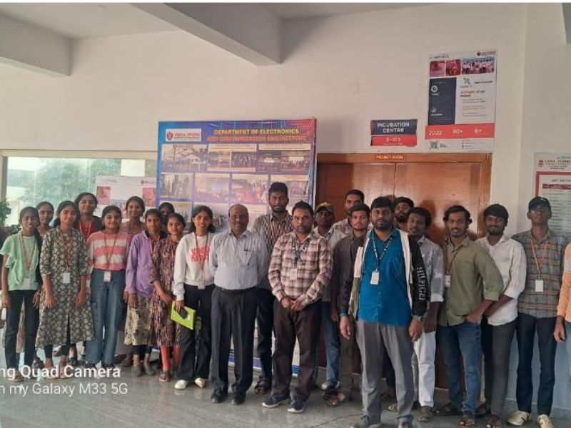
Organized by: Department of Electronics and Communication Engineering (ECE), in association with IEEE and ISF-VJIT
Venue: VLSI Laboratory (E103), Department of ECE, Vidya Jyothi Institute of Technology (VJIT), Hyderabad
Duration: 29–31 December 2025
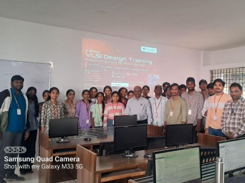
The Department of Electronics and Communication Engineering (ECE), Vidya Jyothi Institute of Technology (VJIT), in association with IEEE and ISF-VJIT, successfully organized a Three-Day VLSI Design Training Program on Verilog HDL, FPGA and EDA Tools from 29th to 31st December 2025. The programme aimed to equip students with fundamental knowledge and hands-on experience in VLSI design methodologies, Verilog Hardware Description Language (HDL), FPGA implementation, and Electronic Design Automation (EDA) tools widely used in the semiconductor industry.
The training programme was coordinated by Dr. M. Krishnaiah, Associate Professor, Department of ECE, who played a pivotal role in planning and organizing the event. The technical sessions were delivered by Mr. G. Ravi Kishore, Mrs. T. Swapna Rani, and Mr. J. Prakash, Assistant Professors from the Department of ECE, who combined theoretical concepts with extensive practical demonstrations and laboratory exercises.
The inaugural session introduced participants to the fundamentals of Very Large Scale Integration (VLSI) technology, its significance in modern electronic systems, and the latest trends in the semiconductor industry. Students gained an overview of the complete VLSI design flow, design challenges, emerging technologies, and career opportunities in VLSI and embedded systems.
On the first day, participants were introduced to the fundamentals of Verilog Hardware Description Language (HDL). The sessions covered modules, ports, operators, data types, procedural blocks, and various modeling styles, including behavioral, dataflow, and structural modeling. Students learned how digital circuits are described, simulated, and verified using Verilog HDL through interactive demonstrations and coding exercises.
The second day focused on the design and implementation of combinational and sequential digital circuits using Verilog HDL. Participants gained practical experience in designing multiplexers, decoders, counters, finite state machines (FSMs), and arithmetic circuits. The sessions also emphasized test bench development, simulation, debugging methodologies, and verification using industry-standard EDA tools.
The third day was dedicated to FPGA architecture and implementation techniques. The resource persons demonstrated the complete FPGA design flow, including synthesis, implementation, constraint specification, timing analysis, hardware verification, and resource utilization. Through hands-on laboratory sessions, students implemented their Verilog designs on FPGA platforms and observed real-time hardware execution, enabling them to bridge the gap between software simulation and physical implementation.
Throughout the three-day programme, participants actively engaged in coding exercises, laboratory experiments, simulations, design demonstrations, and interactive discussions. The practical orientation of the training significantly enhanced students’ understanding of digital system design while exposing them to current industry practices and design methodologies.
The valedictory session concluded with participant feedback, during which students appreciated the comprehensive curriculum, practical learning approach, and guidance provided by the resource persons. Certificates were distributed to all participants upon the successful completion of the training programme.
Resource Persons
- Mr. G. Ravi Kishore, Assistant Professor, Department of ECE
- Mrs. T. Swapna Rani, Assistant Professor, Department of ECE
- Mr. J. Prakash, Assistant Professor, Department of ECE
Programme Coordinator
Dr. M. Krishnaiah
Associate Professor, Department of Electronics and Communication Engineering
Objectives
- To introduce students to modern VLSI design methodologies and semiconductor industry practices.
- To provide hands-on training in Verilog HDL programming and digital circuit design.
- To familiarize participants with FPGA architecture and implementation techniques.
- To expose students to industry-standard Electronic Design Automation (EDA) tools.
- To develop practical skills in digital design, simulation, verification, and hardware implementation.
Topics Covered
Day 1: Introduction to VLSI and Verilog HDL
- Fundamentals of VLSI Design
- VLSI Design Flow
- Introduction to Verilog HDL
- Data Types and Operators
- Behavioral, Dataflow, and Structural Modeling
- Simulation Fundamentals
Day 2: Digital Design Using Verilog HDL
- Combinational Circuit Design
- Sequential Circuit Design
- Counters and Finite State Machines (FSMs)
- Test Bench Development
- Simulation and Debugging Techniques
Day 3: FPGA and EDA Tools
- FPGA Architecture and Applications
- Synthesis and Implementation Flow
- Timing Analysis and Optimization
- Hardware Verification
- Hands-on FPGA Design Demonstration
Programme Outcomes
Upon successful completion of the training programme, participants were able to:
- Understand the complete VLSI design flow from specification to implementation.
- Develop and simulate digital circuits using Verilog HDL.
- Perform functional verification using Electronic Design Automation (EDA) tools.
- Implement and validate digital designs on FPGA platforms.
- Analyze timing performance and hardware resource utilization.
- Apply VLSI design concepts to academic projects, research activities, internships, and industry-oriented applications.
Conclusion
The Three-Day VLSI Design Training Program on Verilog HDL, FPGA and EDA Tools successfully provided participants with a strong foundation in digital system design and modern VLSI development methodologies. The effective blend of theoretical instruction, practical laboratory sessions, and FPGA implementation enabled students to acquire industry-relevant technical skills and enhanced their readiness for advanced studies, research, internships, and rewarding careers in the rapidly expanding semiconductor, VLSI, and embedded systems industries.








0 Comments