
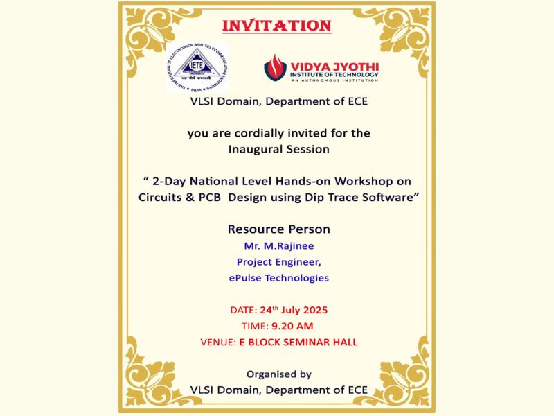
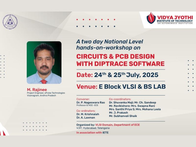
Dates: 24–25 July 2025
Organized by: VLSI Domain, Department of Electronics & Communication Engineering, VJIT
In Association with: IETE Student Forum (ISF)
Resource Person: Mr. M. Rajinee, Project Engineer, ePulse Technologies
Introduction
The VLSI Domain of the Department of Electronics & Communication Engineering, Vidya Jyothi Institute of Technology (VJIT), in association with the IETE Student Forum (ISF) and ePulse Technologies, successfully organized a Two-Day National-Level Hands-on Workshop on Circuits & PCB Design on 24th and 25th July 2025.
Conducted exclusively for third-year ECE students, the workshop focused on developing practical skills in Printed Circuit Board (PCB) design using DipTrace software. The programme combined expert lectures with extensive hands-on practice, enabling participants to understand the complete PCB design workflow—from schematic creation to PCB layout, 3D visualization, and manufacturing file generation.
Objectives
The workshop was organized with the following objectives:
- Introduce students to professional PCB design techniques and best practices.
- Develop proficiency in schematic design and PCB layout using DipTrace.
- Familiarize participants with PCB structures, IPC standards, and multilayer PCB concepts.
- Provide practical exposure to PCB manufacturing processes and design verification.
- Enable students to design industry-standard PCBs for minor and major academic projects.
- Bridge the gap between theoretical electronics and real-world hardware implementation through hands-on learning.
Workshop Structure
The workshop was carefully designed to provide a balanced combination of theoretical knowledge and practical application across two intensive days.
Day 1 – Introduction to PCB Design
The first day focused on the fundamentals of PCB design and introduced participants to the concepts required for professional circuit development.
Topics covered included:
- Introduction to Printed Circuit Boards (PCB) and their industrial applications
- PCB structure and IPC standards
- Electronic components and component identification
- Types of PCBs and mounting/assembly techniques
- Hierarchical design methodology
- Materials used in PCB fabrication
- Vias and PCB panelization
- Signal integrity concepts
- Complete PCB design workflow
Day 2 – Circuit Design and Manufacturing Process
The second day emphasized practical implementation using DipTrace software. Participants learned the complete design flow from schematic capture to manufacturing-ready PCB files.
Sessions included:
- Introduction to the DipTrace design environment
- Schematic capture and circuit design
- PCB component placement and routing
- 3D PCB visualization
- Generation of Gerber files and NC Drill files for manufacturing
- PCB verification and design optimization
Hands-on Learning Experience
The practical sessions formed the highlight of the workshop. Participants designed and simulated real electronic circuits using DipTrace software before converting them into professional PCB layouts.
Students successfully completed several design exercises, including:
- 12V to 5V DC Power Supply Circuit
- Full Adder Circuit using two Half Adders
- Hierarchical schematic design
- PCB placement and routing
- Dual-layer trace connections
- 3D PCB model generation
- Gerber and NC Drill file generation for fabrication
During the laboratory sessions, participants also learned troubleshooting techniques for common PCB design challenges, including routing optimization and top/bottom layer connectivity.
Participant Engagement
The workshop witnessed enthusiastic participation from 150 third-year Electronics & Communication Engineering students.
Interactive discussions, live demonstrations, and one-to-one mentoring enabled participants to clarify concepts and strengthen their understanding of PCB design methodologies. The resource person provided continuous guidance throughout the practical sessions, ensuring that every participant successfully completed the assigned design exercises.
Feedback collected from participants reflected high levels of satisfaction, with students appreciating the structured curriculum, practical exposure, and industry-oriented learning approach.
Workshop Outcomes
Upon completion of the workshop, participants were able to:
- Identify and understand various electronic components used in PCB design.
- Design and develop electronic circuits using professional PCB design software.
- Understand the complete electronics product development workflow.
- Gain practical experience in PCB layout, routing, and manufacturing preparation.
- Generate manufacturing-ready Gerber and NC Drill files.
- Apply PCB design concepts effectively in minor and major academic projects.
- Improve their technical problem-solving and hardware design skills.
Future Recommendations
Based on participant feedback, the following recommendations were proposed for future editions of the workshop:
- Conduct advanced workshops on multilayer and high-speed PCB design.
- Include PCB simulation and signal integrity analysis.
- Organize fabrication and PCB assembly demonstrations.
- Introduce industry-oriented certification programmes.
- Incorporate more real-world design projects and case studies.
Conclusion
The Two-Day National-Level Hands-on Workshop on Circuits & PCB Design was a highly successful technical initiative that strengthened participants’ understanding of modern PCB design methodologies and electronic hardware development.
The collaboration between the Department of Electronics & Communication Engineering, the IETE Student Forum, and ePulse Technologies provided students with valuable industry exposure and practical experience in professional PCB design. Through a combination of expert guidance, interactive sessions, and intensive hands-on practice, participants developed the confidence and technical competence required to design high-quality electronic circuits for academic projects and future engineering careers.
The workshop effectively bridged the gap between theoretical learning and practical implementation, empowering students with industry-relevant skills in PCB design, manufacturing, and product development.








0 Comments