
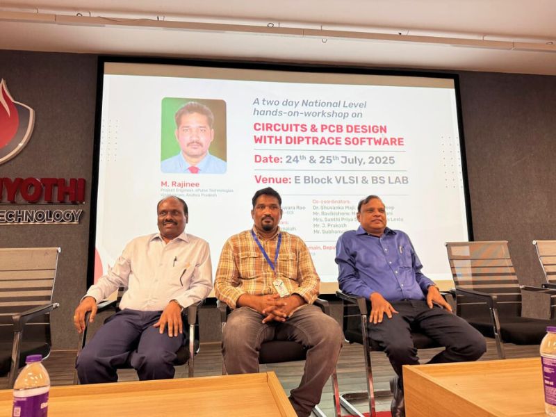
A Two-Day National Level Hands-on Workshop on Circuits & PCB Design
Date: 24th and 25th July, 2025
Organized By: VLSI Domain, ECE In association with IETE Student Forum (ISF)
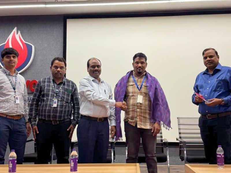
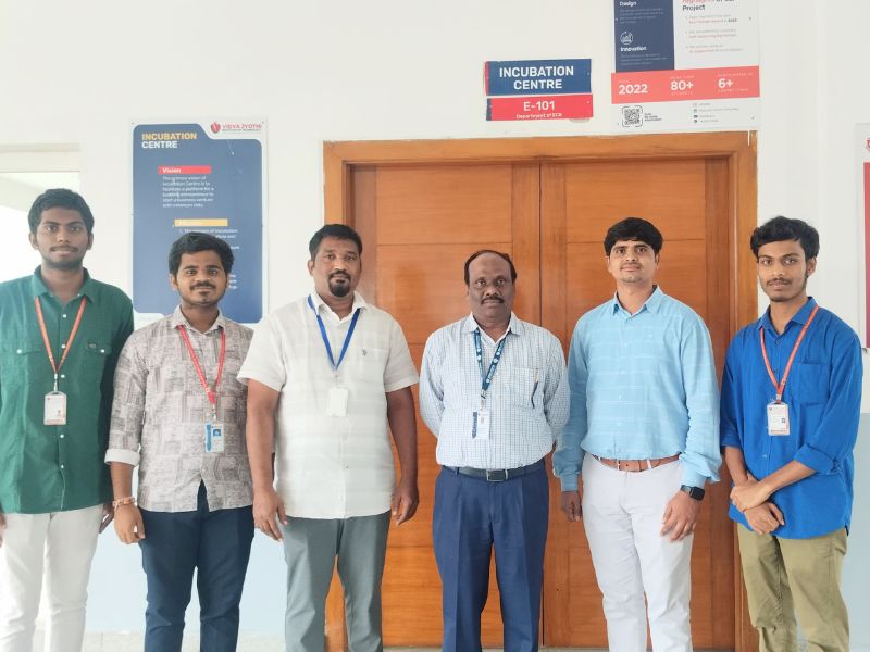
Resource Person: Mr. M. Rajinee, Project Engineer, ePulse Technologies.
Objective: This workshop was about the techniques and best practices. This course showed how students can design boards more effectively and produce professional results. This “Printed Circuit Board Design” workshop included with schematic examples of circuits diagrams and PCB designs of same, and it covered PCB structure, PCB design aspects, Multilayer high speed PCB designs, library creation, etc. & also it is going to help the students to develop professional grade PCB for their Major/Minor projects. To increase the impact and effectiveness of the workshop, as far as possible lectures followed by hands on practice sessions were planned.
Introduction: A Two-Day National-Level Hands-on Workshop on Circuits and PCB Design using DipTrace software was collaboratively organized by the VLSI Domain, Department of ECE, Vidya Jyothi Institute of Technology, in association with ePulse Technologies. The workshop, conducted in offline mode on July 24th and 25th, 2025, was exclusively designed for third-year students
Workshop Structure and Content
The workshop was carefully designed to ensure a balanced learning experience, consisting of both theoretical sessions and hands-on practical activities.
Day 1: Introduction to PCB Design
The first day set the stage for an immersive learning experience. Theoretical sessions introduced participants to the fundamentals of PCB design.
- Overview of Printed Circuit Board (PCB) design and its applications across industries.
- Introduction to PCB structure and IPC standards.
- Types of electronic components and their identification
- PCB types and Mounting /Assembly techniques
- Hierarchy Method
- Materials used for PCB Design
- Vias and PCB panelizing
- Signal Integrity
- PCB Design flow
Day 2: Circuit Design and Manufacturing process
The second day aimed to enhance the participants’ understanding by introducing the DipTrace software workflow. Sessions began with an introduction to schematic capture and PCB layout, including the generation of Gerber files and NC drill files.
- Introduction to diptrace software design flow.
- Design various schematic of Circuit
- PCB Layout for placement and routing
- Layout converted to 3D model PCB
- Generating of Gerber file and NC drill file for manufacturing PCB Board.
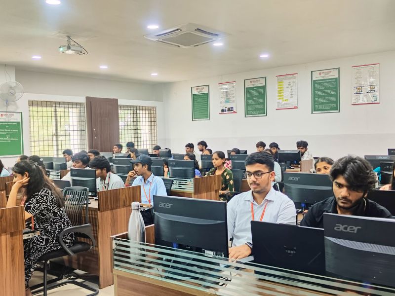
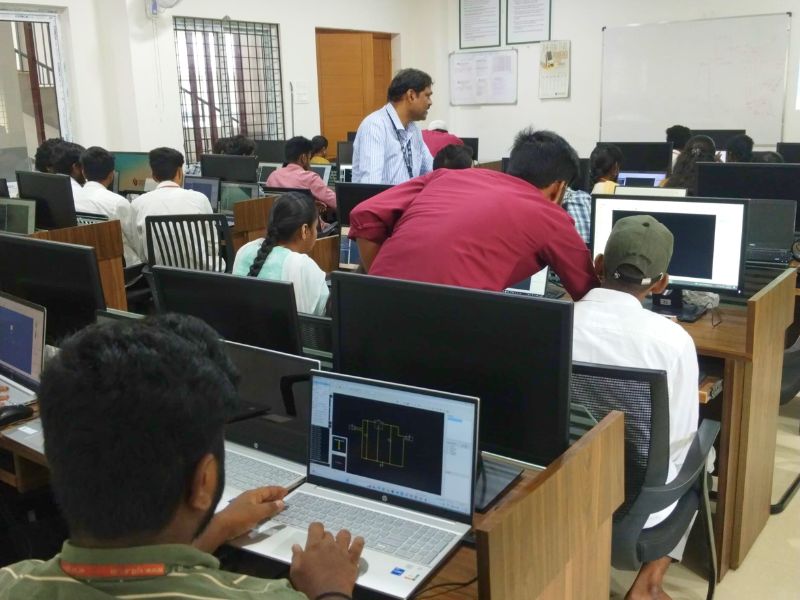
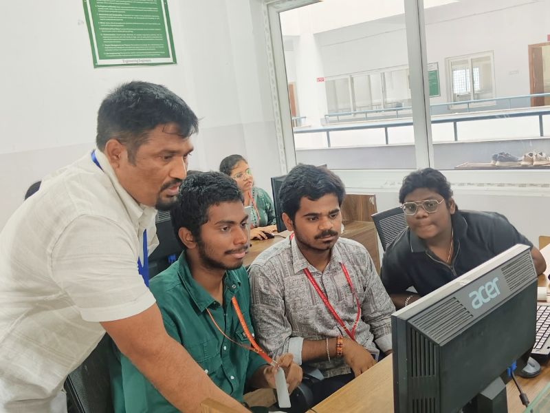
Hands-on Sessions and Practical Learning
The hands-on sessions formed the core of the workshop. Participants used Diptrace software to design various circuits and convert them into PCB layout, The participants designed a 12V to 5V DC power supply and a full adder circuit using two half adders with the hierarchical method, among other exercises. Gaining practical experience in 3D PCB modeling and troubleshooting common issues, such as connecting traces to components on both the top and bottom layers.
Participant Engagement and Feedback
The workshop witnessed enthusiastic participation from 150 third-year ECE students. Interactive discussions allowed students to clarify doubts and share their perspectives on Printed Circuit Board (PCB) Design. Facilitators provided step-by-step guidance during the practical sessions, ensuring all participants gained a solid understanding of the concepts. Feedback collected from students highlighted their appreciation for the well-structured content, practical exposure, and personalized mentorship.
Outcome and Impact
- Knowledge and Identification of Electronic Components
- Hands-on experience of working with PCB Design.
- Understanding of Electronics Project Design Flow.
- Experience of Best learning practice
- Exposure to complete PCB Design & manufacturing process.
- Acquire skills to do better Minor/Major Projects
Future Recommendations
Based on participant feedback, the following recommendations were made for future workshops:
- Advanced PCB Design, Simulation & Manufacturing Process
- Offer more hands-on projects and real-world case studies.
- Conduct certification-based workshops for career enhancement.
Conclusion
The PCB Design Workshop at Vidya Jyothi Engineering College was a resounding success, achieving its goal of imparting practical knowledge and fostering technical growth. The collaboration with ePulse Technologies provided students with exposure to the latest technologies in the PCB Design and Manufacturing Techniques, participants are well-equipped to contribute to the technological advancements of the future.


0 Comments